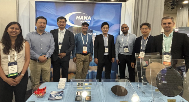
Hana Micron , a semiconductor post-processing specialist, announced on the 12th that it participated in the '2025 Electronic Components and Technology Conference (ECTC)' held in Texas, USA and introduced its next-generation high-performance semiconductor packaging solution.
ECTC is the world's largest electronics packaging technology conference hosted by the Electronic Packaging Society under the Institute of Electrical and Electronics Engineers (IEEE), and this year marks its 75th anniversary. This event was attended by over 2,000 experts from 20 countries around the world, and global semiconductor companies such as TSMC, Intel, IBM, ASE, and Sony participated in large numbers to share the latest technologies and research results.
Hana Micron participated in this ECTC as a gold sponsor and operated an exhibition booth, and unveiled its main product portfolio including wafer-level package (WLP), flip-chip BGA (FCBGA), system in package (SiP), and bridge die-based 2.xD packaging.
The packaging structure announced by Hana Micron is a next-generation 2.xD packaging technology (HICTM) that utilizes bridge dies and copper posts to optimize signal and power transmission. It complements the limitations of the existing TSV (Through-Silicon Via) method and has been recognized as a technology suitable for AI and HPC (High-Performance Computing) fields by showing effects such as shortening data transmission distance, reducing RC (RC delay), and improving power efficiency.
A company official said, “Through this ECTC participation, we were able to share our technological prowess and vision with global technology leaders,” and “We will continue to strengthen our competitiveness in the global packaging market through continuous technological advancement and customer cooperation.”
- See more related articles
You must be logged in to post a comment.