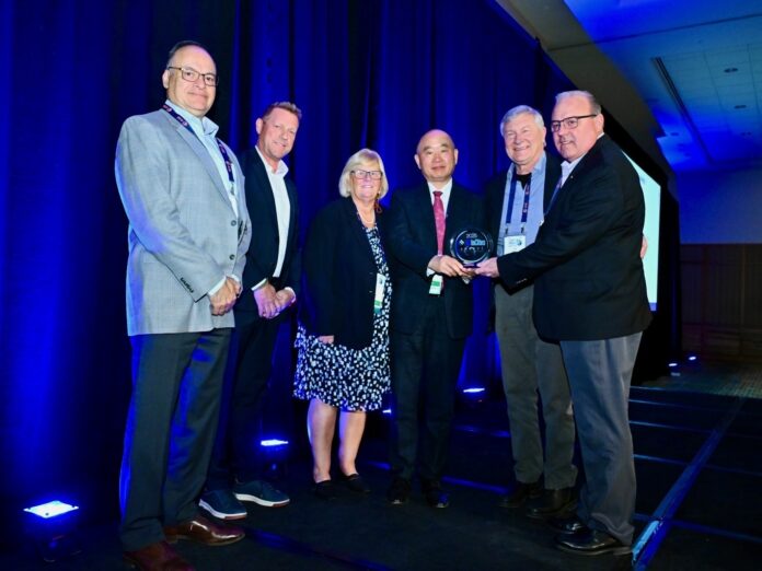
ACM Research, Inc. (NASDAQ: ACMR), a leading provider of wafer and panel processing solutions for semiconductor and advanced wafer-level packaging (WLP) applications, announced that its Ultra C ECP ap-p tool has won a Technology Enablement category award at the 2025 3D InCites Awards. The award recognizes companies that have driven industry progress with cutting-edge solutions and innovations by identifying and solving critical challenges in advancing heterogeneous integration roadmaps.
Designed for fan-out panel-level packaging (FOPLP), ACM’s Ultra C ECP ap-p system is the first commercial high-volume copper deposition system for the large-panel market. The system uses a horizontal plating process to achieve exceptional uniformity and precision across the entire panel. The equipment can process panels measuring 515 mm x 510 mm and 600 mm x 600 mm and can be used for plating steps in a variety of processes, including filler, bump and redistribution layers.
“We believe this 3D InCites award is recognition of ACM’s commitment to solving our customers’ challenges in panel-level packaging (PLP),” said Dr. David Wang, ACM President and CEO. “With the increasing demand for larger chiplets, high-performance graphics processing units (GPUs) and high-density, high-bandwidth memory (HBM), PLP has emerged as a key solution for reducing cost and improving efficiency. The Ultra C ECP ap-p system is a key addition to ACM’s expanding FOPLP portfolio and reinforces our commitment to advancing high-volume manufacturing solutions.”
◆ ACM's FOPLP portfolio is as follows:
- Ultra C ECP ap-p for copper deposition
- Ultra C vac-p for flux cleaning
- Ultra C bev-p for bevel etching and cleaning
The 3D InCites Award winners, announced at the IMAPS Device Packaging Conference, were selected for their outstanding contributions to advancing the heterogeneous integration roadmap.
- See more related articles
You must be logged in to post a comment.